Band anti-crossing model in dilute-as ganas alloys
- Select a language for the TTS:
- UK English Female
- UK English Male
- US English Female
- US English Male
- Australian Female
- Australian Male
- Language selected: (auto detect) - EN
Play all audios:

ABSTRACT The band structure of the dilute-As GaNAs material is explained by the hybridization of localized As-impurity states with the valance band structure of GaN. Our approach employs the
use of Density Functional Theory (DFT) calculated band structures, along with experimental results, to determine the localized As-impurity energy level and coupling parameters in the band
anti-crossing (BAC) _k ∙ p_ model for N-rich alloys. This model captures the reduction of bandgap with increasing arsenic incorporation and provides a tool for device-level design with the
material within the context of the _k ∙ p_ formalism. The analysis extends to calculating the effect of the arsenic impurities on hole (heavy, light and split-off) effective masses and
predicting the trend of the bandgap across the entire composition range. SIMILAR CONTENT BEING VIEWED BY OTHERS AN INNOVATIVE TECHNIQUE FOR ELECTRONIC TRANSPORT MODEL OF GROUP-III NITRIDES
Article Open access 30 October 2020 IR IMPURITIES IN \(\ALPHA\)- AND \(\BETA\)-\(\TEXT {GA}_{2}\TEXT {O}_{3}\) AND THEIR DETRIMENTAL EFFECT ON P-TYPE CONDUCTIVITY Article Open access 26 May
2023 BANDGAP AND REFRACTIVE INDEX ESTIMATES OF INALN AND RELATED NITRIDES ACROSS THEIR FULL COMPOSITION RANGES Article Open access 01 October 2020 INTRODUCTION Major breakthroughs in
solid-state lighting and energy efficiency applications have been enabled in recent decades through thorough investigation of the class of III-nitride semiconductors, including GaN, InN,
AlN, and their alloys with one another1,2. Advancements in both material epitaxy methods, along with new, innovative approaches for device level design, have enabled the production of highly
efficient light emitting diodes (LED) devices3,4. Refined understanding of intrinsic material properties of this semiconductor family has enabled their use in various applications, such as
high-speed electronics, lasers, and solar energy applications5,6,7. A key feature of the III-nitride semiconductors is their direct bandgap property, which is required for use in
energy-efficient light-emitting applications. The materials also possess other useful optoelectronic, chemical, and tribological properties, which allow them to be applied in a wide variety
of devices and applications8,9. In contrast to the substantial work towards investigating the family of III-nitride semiconductors, with prime examples being the InGaN and AlGaN alloys10,
much less literature has been published on the dilute-anion III-nitride semiconductor alloys. Recent work has illustrated the potential of using the dilute-arsenic GaNAs alloy for achieving
a broad range of bandgaps across the entire visible spectrum11,12,13. Analysis also indicates that the material is promising due to its reduced Auger recombination rate in comparison to
GaN14, making it a strong candidate for use in future optoelectronic applications. The first reported incorporation of arsenic into a GaN crystal was reported by Li and co-workers via the
metalorganic chemical vapor deposition (MOCVD) growth technique12. Incorporation of ~6.7% As-content via MOCVD was later reported by Kimura and co-workers13. Additionally, GaNAs alloys
across the entire As-composition have been grown using the molecular beam epitaxy (MBE) technique by Yu and co-workers15,16,17. These experiments indicate that the GaNAs material exhibits an
increasing reduction of the bandgap from that of GaN with higher arsenic incorporation, indicating an experimental pathway towards tunability of the bandgap and other electronic properties
by controlling the impurity incorporation. Thus, as implementing the GaNAs material into future device design may prove important, an accurate description of the band structure in the
context of the _K ∙ P_ perturbation theory for device-modeling purposes is instrumental. Previous studies have shown that the band anti-crossing (BAC) model can be applied as a technique to
specifically describe the band structures of highly-mismatched semiconductor alloys18. Specifically, the band anticrossing model has been widely used in the _K · P_ method to investigate the
electronic properties of highly-mismatched alloyed semiconductors, including III-V alloys such as dilute-N GaAsN and InGaAsN19,20, dilute-N GaPN20, dilute-N AlGaNAs21, and others22,23,24,
along with various IV-class semiconductors25, and II-VI semiconductors26,27,28. The various models used for different material systems involve modifying the Hamiltonian to introduce
localized energy levels associated with the dilute-ion incorporation of a new element into the host semiconductor material. As part of the highly-mismatched semiconductor alloy class, the
BAC model can be potentially useful for analyzing the band structure of the dilute-As GaNAs alloys. Developing the band anticrossing model for dilute-As GaNAs alloys would provide a key step
towards understanding the band structure evolutions of the alloy and providing a more accurate band structure analysis for device design purpose in the future. Using DFT results to fit our
model allows for the atomistic description of the electronic states in the material to be transformed into useful parameters for nanoscale device level design. In this work, we develop a
valence-band hybridization BAC model to determine the characteristics of the electronic structure and properties for dilute-As GaNAs alloys. The BAC parameters (_C__GaNAs_ and _E__As_) of
the electronic structure of the GaN1−xAsx material system with As-content ranging from 0% up to 12.5% are evaluated and presented. The effect of the BAC interaction on the band dispersions
of the GaN1−xAsx alloys are analyzed. Our findings indicate the validity of using valence-band hybridization BAC model to explain the significant electronic band structure modifications in
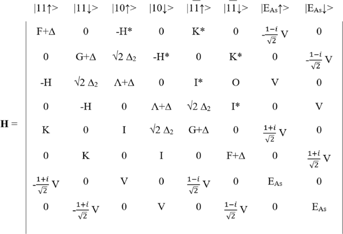
dilute-As GaNAs alloys when compared to the GaN binary alloy. COMPUTATIONAL METHOD A 6-band Hamiltonian from _K ∙ P_ perturbation theory is commonly used to model the valence band electronic
structure of binary wurtzite semiconductors29. The eigensolutions of this Hamiltonian are doubly degenerate and split into 3 distinct energy bands, known as the heavy hole (HH), light hole
(LH), and split-off (SO) bands. The energy dispersions of these bands are calculated as a function of wave vector near the gamma point (_K_ = 0). Use of the correct material parameters
provides an accurate description of the band structure at this band edge (near Γ-point), which can then be used in self-consistent analysis to calculate the spontaneous emission rate, gain
properties, and other important characteristics of the resultant quantum well structures30. For the ternary dilute-anion GaNAs material system, the traditional 6-band _K ∙ P_ Hamiltonian
used to model the valence band of GaN is extended by including two additional states that represent the localized impurity level energy _E__As_, as shown in Fig. 1. This is known as the
valence band anticrossing model31. The localized energy state is used to modify the original GaN host energy bands with band edges set using the virtual crystal approximation (VCA) between
GaN and GaAs. The hybridization energy _V_, which describes how strongly the localized state perturbs the host states, is given by the hybridization energy parameter _C__GaNAs_ and assumes a
square-root dependence on the impurity concentration. More remote states are neglected due to their large distances from the valence band maximum of GaN. In the Hamiltonian from Fig. 1, the
parameters can be defined using the following equations: $$\begin{array}{c}{\rm{\Delta }}={E}_{v}(x)-[{{\rm{\Delta }}}_{1}(x)+{{\rm{\Delta }}}_{2}(x)]\,\end{array}$$ (1)
$$\begin{array}{c}F={{\rm{\Delta }}}_{1}(x)+{{\rm{\Delta }}}_{x}(x)+\,\lambda +\theta \,\end{array}$$ (2) $$\begin{array}{c}G={{\rm{\Delta }}}_{1}(x)-{{\rm{\Delta }}}_{x}(x)+\,\lambda
+\theta \end{array}$$ (3) $$\begin{array}{c}\,\lambda ={A}_{1}{k}_{z}^{2}+{A}_{2}{k}_{t}^{2}+{D}_{1}{\varepsilon }_{zz}+{D}_{2}({\varepsilon }_{xx}+{\varepsilon }_{yy})\end{array}$$ (4)
$$\begin{array}{c}\theta ={A}_{3}{k}_{z}^{2}+{A}_{4}{k}_{t}^{2}+{D}_{3}{\varepsilon }_{zz}+{D}_{4}({\varepsilon }_{xx}+{\varepsilon }_{yy})\end{array}$$ (5)
$$\begin{array}{c}H=i{A}_{6}{k}_{z}{k}_{t}-{A}_{7}{k}_{t}\end{array}$$ (6) $$\begin{array}{c}I=i{A}_{6}{k}_{z}{k}_{+}+{A}_{7}{k}_{+}\end{array}$$ (7)
$$\begin{array}{c}K={A}_{5}{k}_{+}^{2}\end{array}$$ (8) $$\begin{array}{c}V={C}_{GaNAs}\sqrt{x}\end{array}$$ (9) where the wave vector terms are represented as:
$$\begin{array}{c}{k}_{t}=\sqrt{{k}_{x}^{2}+{k}_{y}^{2}}\end{array}$$ (10) $$\begin{array}{c}{k}_{+}={k}_{x}+i{k}_{y}\end{array}$$ (11) and the virtual crystal approximation terms from eqs
(1–3) are: $$\begin{array}{c}{E}_{v}(x)=({E}_{g,GaN}-{E}_{g,GaAs})\cdot x\end{array}$$ (12) $$\begin{array}{c}{{\rm{\Delta }}}_{1}(x)={{\rm{\Delta }}}_{1,GaN}\,\ast \,(1-x)+\,{{\rm{\Delta
}}}_{1,GaAs}\cdot x\end{array}$$ (13) $$\begin{array}{c}{{\rm{\Delta }}}_{2}(x)={{\rm{\Delta }}}_{2,GaN}\,\ast \,(1-x)+{{\rm{\Delta }}}_{2,GaAs}\cdot x\end{array}$$ (14) The material
parameters used in the relations above are presented in Table 1. The bandgaps and band edge (crystal field and split-off) energies of the binary endpoint materials, GaN and GaAs, are used in
the virtual crystal approximation terms. The virtual crystal approximation assumes a linear interpolation of the band edges between the binary materials. The effective mass parameters are
not interpolated; the parameters for GaN are used for analyzing the perturbative effect arsenic concentration has on band dispersions and effective mass. The eigenenergies of the Hamiltonian
in Fig. 1 are evaluated at the gamma (Γ) point as a function of _x_ (As-content) and the BAC parameters (_E__As_ and _C__GaNAs_). Diagonalizing the Hamiltonian reveals a restructuring of
the valance band into four doubly-degenerate bands, denoted as _E__As−like_, _E__A−like_, _E__B−like_, and _E__C−like_, respectively. The first band, _E__As−like_, is a newly formed energy
band by the interaction of the arsenic states with the host GaN states, whereas the other bands correspond to the GaN-perturbed HH, LH, and SO bands, respectively. For _x_ > 0,
_E__As−like_ emerges as a new valence band maximum (VBM), and the fundamental bandgap of the material is denoted as the difference in energy between the conduction band minimum energy of GaN
and this new VBM. One can then find the optimal set of BAC parameters that reach a minimum of the error between the BAC bandgap as a function of _x_ versus a separate theoretical
calculation or experimental measurement of the bandgap. Suitable BAC parameters for the dilute-As GaNAs ternary alloy system can be found by comparing the BAC band gap to that of
First-Principle Density Functional Theory (DFT) calculations. First-Principles DFT calculations were performed by using the Projector Augmented Wave (PAW) method using the Local Density
Approximation (LDA) exchange-correlation potential in the MedeA VASP software. The scissor operator was used to correct for errors in the bandgap calculation32. Although the use of the LDA
is known to introduce some errors into the band structure calculations33,34, particularly in the effective masses, only the bandgap as a function of arsenic content is used on our
calculation. Supercells of gallium and nitrogen atoms were developed with a substitution of a single As on an N site, thereby changing the GaN supercell into a GaNAs supercell. Details of
the computational method and results can be found in previous publications11. RESULTS AND DISCUSSION The localized energy _E__As_ was varied from −0.8 eV to 0.8 eV in 0.01 eV increments
while the hybridization energy _C__GaNAs_ was varied from 0 eV to 3 eV in the same increments. These were used as fitting parameters to minimize the error between the DFT-calculated band
gaps and the resultant bandgaps from the diagonalized Hamiltonian. Figure 2(a–d) show selected BAC parameter sweeps of the _K ∙ P__-_modelled reduction of energy bandgap against the DFT
calculations. The effect on the bandgap reduction of the four _E__As_ values are shown. This comparison shows that the _E__As_ value for the dilute-As GaNAs is lying slightly below the
valence band maximum of the GaN. The dilute-As GaNAs material system is best-modelled with the parameters of localized impurity energy at _E__As_ = −0.39 eV (below the VBM of GaN) and a
coupling constant _C__GaNAs_ = 2.57 eV. The BAC-calculated subband transition energies at the gamma point with these energy parameters are presented in Fig. 3. An interesting feature
revealed in the transition energies in Fig. 3 is the drastic increase of the split-off energy as a function of _x_. The model predicts large split-off energies (>1 eV), compared to both
that of GaN30 and GaAs35, at even low levels of arsenic incorporation (~1.56%). This prediction is supported by the DFT-calculations11, which also indicate a large splitting of the split-off
band from the heavy hole and light hole bands in the dilute-As regime. The previously described method of determining the BAC parameters was also performed on experimental measurements of
the bandgap of epitaxial GaNAs films reported by Kimura _et al_.13 This dataset is very-well fit by the BAC model, using the same GaN and GaAs parameters as those in Table 1, except the
different value of GaN band gap of _E__g_,_GaN_ = 3.39 eV, as measured in the experiment. Figure 4 presents the best fit found using the BAC parameters _E__As_ = −0.32 eV and _C__GaNAs_ =
2.64 eV. Both coupling constants (_E__As_ and _C_GaNAs) are in close agreement with those obtained via the DFT calculations, within a value of 0.1 eV between the DFT and experimental
results. This provides assurance that these values of the parameters reasonably model the reduction bandgap in the N-rich valence band hybridization BAC model. Previous work on the N-rich
GaN1−xAsx valence band hybridization BAC model done by Wu _et al_.31 suggested BAC parameters of _E__As_ = 0.62 eV and _C__GaNAs_ = 0.75 eV. These values differ drastically from our results
and predict a positive _E__As_, placing the newly-formed valence subband to be above the VBM of GaN. Moreover, an important aspect of our parameters is that they accurately predict the
bandgap in the dilute limit (as _x_ → 0) to approach that of GaN (~3.4 eV). As indicated in Fig. 2, impurity energy levels above the VBM will cause the bandgap calculated from the
Hamiltonian to approach the value of _E__g_,_GaN_ − _E__As_ in the dilute limit. Use of localized energies below the VBM resolves this issue while providing a good fit to the reduction of
the bandgap in the target composition range. The discrepancy between the values reported in this report and the previous work can be potentially explained by the nature of the growth
conditions and how the arsenic atoms are incorporated into the alloy. It is known that the fabrication of GaNAs alloys by MBE is highly dependent upon the growth conditions. Arsenic-doped
gallium nitride (_x_ ~ 0.002) samples grown under gallium-rich conditions exhibit a broad PL at around 2.6 eV (~0.8 eV below that of GaN), whereas films grown under nitrogen-rich conditions
(with the same arsenic flux) exhibit a much smaller shift from the gallium nitride peak to a value around 3.34 eV (less than 0.1 eV from GaN)36. This fact, in conjunction with the fact that
the DFT-calculated bandgaps of the minimally clustered, single crystal material approaches GaN in the dilute limit, suggests that it is necessary to achieve high nitrogen to gallium ratios
to promote crystalline GaNAs alloy growth. The bandgap of alloys grown under gallium-rich conditions may be attributed to transitions involving vacancy defects rather than being a transition
associated with a true alloy state. Further experimental and theoretical analysis into the nature of arsenic-doped GaN and phase-separation in dilute-As GaNAs films is necessary to
understand the nature of the bandgap in this very dilute limit. A prediction of the bandgap across a greater composition range of the ternary alloy GaN1-xAsx from GaN (_x_ = 0) to GaAs (_x_
= 1) can be achieved by using a quasi-linear interpolation between the valence BAC model on the dilute-anion side and the conduction BAC model on the dilute-cation side31. This interpolation
is achieved using the equation: $$\begin{array}{c}{E}_{g}(x)=(1-x)\cdot {E}_{g,N-rich}(x)+x\cdot {E}_{g,As-rich}(x)\end{array}$$ (15) Such an interpolation, through the regime in which the
alloy is expected to be in wurtzite configuration with minimal-clustering, is presented in Fig. 5 using our DFT-calculated valence BAC parameters of _E__As_ = −0.39 eV, _C__GaNAs_ = 2.57 eV,
and known conduction BAC parameters of _E__N_ = 1.63, _E__GaAsN_ = 2.7 eV15,16,17. By inserting wave vector dependence into the Hamiltonian, the effect of the arsenic impurity on the band
dispersions can be determined. The valence subband dispersions of unstrained GaN were calculated by the 6-band _K ∙ P_ model, without the valence BAC effect, using the parameters for the
material listed in Table 1. Furthermore, the valence subband dispersions of GaN0.9844As0.0156 and GaN0.9375As0.0625 were determined from the 8-band valence BAC _K ∙ P_ model using the
DFT-fit BAC parameters and the GaN effective mass parameters from Table 1. These dispersions are presented in Fig. 6. It is evident that the valence band structure of the GaNAs alloy is
heavily perturbed by the presence of the localized impurity. Most notable is the existence of a new, relatively heavy valence band maximum that originates from the _E__As−like_ eigenstate,
despite the use of the _E__As_ localized energy below the valence band maximum of GaN. The transition between this state and the conduction band of GaN is responsible for the fundamental
bandgap of the alloy. A strong interaction occurs between this state and the GaN split-off band, resulting in a large deepening of the split-off band energy at even low arsenic
concentrations, along with an increase of the effective mass of this subband. The heavy hole and light hole bands remains close in energy at the gamma point, increasing in energy slowly
according to the virtual crystal approximation. Nevertheless, the character of these dispersions demonstrates a strong interaction with the arsenic-state, rapidly deviating from the form
predicted by the standard 6-band model for wurtzite semiconductors. This indicates that the use of the band anti-crossing model in device-model applications can have profound deviations from
using a more simplistic 6-band valence band model of GaNAs which assumes no deviation in the wave vector dependence. Near the gamma point, energy bands can be modeled with an effective
mass, which describes the approximate parabolic behavior of the energy well when wave vector is near a minimum. Calculations of the effective mass for each of the valence subbands were
performed by determining the difference in energy between the subband at the gamma point and at very small _K_-space increments in the A (_k__z_) and K (_k__x_) directions. This was
performed using the 6-band model for GaN and the 8-band valence BAC model for GaN1−xAsx in increments of _x_ = 0.005 to _x_ = 0.125, corresponding to the maximum arsenic incorporation of
12.5% investigated in the DFT calculation. The effective masses for each of the subbands in both directions are plotted in Fig. 7. There is a discontinuity between the nature of the GaNAs
subband effective masses from the BAC model in the very dilute limit to those of GaN from the standard 6-band model, even when the same effective mass parameters are used in both
Hamiltonians. This is due to the very strong interaction of the arsenic impurity at even very low incorporation levels, along with the formulation of the Hamiltonian itself. Further
investigation, either theoretical or experimental, into the nature of the band dispersions in this dilute limit will be useful for refining the material parameters. CONCLUSIONS In
conclusion, a band anti-crossing model has been developed for dilute-As GaNAs material system with As-content up to 12.5%. BAC parameters required for the band anticrossing model are
determined by comparing the results from the model with the DFT-calculation findings and experimental findings. The BAC parameters are used in the valence band hybridization _K ∙ P_
perturbation theory to model the effect of an arsenic impurity on the GaN host crystal. Use of a localized impurity energy (_E__As_) below the valence band minimum of GaN is found to
well-model the reduction of bandgap for the material, with the important feature of converging to the bandgap of GaN in the dilute limit. These parameters are essential for device-level
modelling by providing a method to capture the key electronic properties of the alloy, allowing for the detailed design and analysis of green-emitting III-nitride LEDs and other
optoelectronic structures based upon this alloy. REFERENCES * Morkoç, H. Nitride Semiconductor Devices: Fundamentals and Applications (2013). * Nakamura, S. & Fasol, G. (Eds.) _The Blue
Laser Diode_ (1997). * Crawford, M. H. LEDs for Solid-State Lighting: Performance Challenges and Recent Advances. _IEEE J. Sel. Top. Quantum Electron_ 15, 1028–1040 (2009). Article ADS CAS
Google Scholar * Tsao, J. Y. _et al_. Toward Smart and Ultra‐efficient Solid‐State Lighting. _Adv. Opt. Mat._ 2, 809 (2014). Article CAS Google Scholar * Harima, H. Properties of GaN
and related compounds studied by means of Raman scattering. _J. Phys.: Condens. Matter_ 14, R967–R993 (2002). ADS CAS Google Scholar * Zeng, G., Tan, C. K., Tansu, N. & Krick, A.
Ultralow wear of gallium nitride, B. A. _Appl. Phys. Lett_ 109, 051602 (2016). Article ADS Google Scholar * Mishra, U. K., Shen, L., Kazior, T. E. & Wu, Y. F. GaN-based RF power
devices and amplifiers. _Proc. IEEE_ 96, 287 (2008). Article CAS Google Scholar * Wiesmann, C., Bergenek, K., Linder, N. & Schwarz, U. T. Photonic crystal LEDs–designing light
extraction. _Laser & Photon. Rev._ 3(3), 262–286 (2009). Article ADS CAS Google Scholar * Cimalla, V., Pezoldt, J. & Ambacher, O. Group III nitride and SiC based MEMS and NEMS:
materials properties, technology and applications. _O. J. Phys. D: Appl. Phys._ 40, 6386 (2007). Article ADS CAS Google Scholar * Zhao, H., Liu, G., Arif, R. A. & Tansu, N. Current
injection efficiency induced efficiency-droop in InGaN quantum well light-emitting diodes. _Solid State Electron._ 54, 1119–1124 (2010). Article ADS CAS Google Scholar * Tan, C. K. _et
al_. First-principle electronic properties of dilute-As GaNAs alloy for visible light emitters. _Journal of Display Technology_ 9(4), 272–279 (2013). Article ADS MathSciNet CAS Google
Scholar * Li, X., Kim, S., Reuter, E. E., Bishop, S. G. & Coleman, J. J. The incorporation of arsenic in GaN by metalorganic chemical vapor deposition. _Appl. Phys. Lett._ 72(16),
1990–1992 (1998). Article ADS CAS Google Scholar * Kimura, C., Paulson, A., Tang, H. F. & Kuech, T. F. Epitaxial layers with high As content grown by metalorganic vapor phase epitaxy
and their band gap energy. _Appl. Phys. Lett._ 84(9), 1489–1491 (2004). Article ADS CAS Google Scholar * Tan, C. K. _et al_. Auger recombination rates in dilute-As GaNAs semiconductor.
_AIP Adv._ 5(5), 057135 (2015). Article ADS Google Scholar * Yu, K. M. _et al_. Highly mismatched crystalline and amorphous GaN1−xAsx alloys in the whole composition range. _J. Appl.
Phys_., 106, pp. 1-8, Nov. (2009) * Yu, K. M. _et al_. Non-equilibrium GaNAs alloys with band gap ranging from 0.8–3.4 eV, _Physica Status Solidi_ (c), 7(7–8). 1847–1849 (2010). * Yu, K. M.
_et al_. Low gap amorphous alloys grown on glass substrate. _Appl. Phys. Lett._ 97, 1–3 (2010). Google Scholar * Shan, W. _et al_. Band Anticrossing in GaInNAs alloys. _Phys. Rev. Lett._
82(6), 1221–1224 (1999). Article ADS CAS Google Scholar * Lindsay, A. & O’Reilly, E. P. Unification of the Band Anticrossing and Cluster-State models of the Dilute Nitride
Semiconductor Alloys. _Phys. Rev. Lett._ 93(19), 1–4 (2004). Article Google Scholar * Shan, W. _et al_. Band Anticrossing in III-N-V Alloys. _Physica Status Solidi (b)_ 223(1), 75–85
(2001). Article ADS CAS Google Scholar * Shan, W. _et al_. Band anticrossing in dilute nitrides. _J. Phys.: Condens. Matter_ 16(31), 3355–3372 (2004). Google Scholar * Alberi, K. _et
al_. Valence-band anticrossing in mismatched III-V semiconductor alloys. _Phys. Rev. B_ 75, 1–6 (2007). Article Google Scholar * Jefferson, P. H. _et al_. Band anticrossing in GaNxSb1−x.
_Appl. Phys. Lett._ 89, 1–3 (2006). Article Google Scholar * Murdin, B. N. _et al_. Band anticrossing in dilute InNxSb1-x. _Appl. Phys. Lett._ 81(2), 256–257 (2004). Article ADS Google
Scholar * Alberi, K. _et al_. Band anticrossing in SnxGe1-x semiconducting alloys. _Phys. Rev. B._ 77, 1–4 (2008). Article Google Scholar * Walukiewicz, W. _et al_. Interaction of
Localized Electronic States with the Conduction Band: Band Anticrossing in II–VI Semiconductor Ternaries. _Phys. Rev. Lett._ 85(7), 1552–1555 (2000). Article ADS CAS Google Scholar * Yu,
K. M. _et al_. Band anticrossing in group II-Ox-VI1−x highly mismatched alloys, Cd1−xMnyOxTe1−x. _Appl. Phys. Lett._ 80(9), 1571–1573 (2002). Article ADS CAS Google Scholar * Yu, K. M.
_et al_. Dilute II-VI Oxide Semiconductors with Multiple Band Gaps. _Phys. Rev. Lett._ 91(24), 1–4 (2008). Google Scholar * Zhao, H. P. _et al_. Self-consistent gain analysis of type-II ‘W’
InGaN–GaNAs quantum well lasers. _J. Appl. Phys._ 104, 1–7 (2008). Google Scholar * Vurgaftman, I. & Meyer, J. R. Band parameters for nitrogen-containing semiconductors. _J. of Appl.
Phys_ 94, 3680 (2003). Article ADS Google Scholar * Wu, J. _et al_. Valence band hybridization in N-rich GaN1−xAsx alloys. _Phys. Rev. B_ 70, 1–7 (2004). Google Scholar * Fiorentini, V.
& Baldereschi, A. Dielectric scaling of the self-energy scissor operator in semiconductors and insulators. _Phys. Rev. B, Condens. Matter_ 51(23), 17196–17198 (1995). Article ADS CAS
Google Scholar * Kim, Y. S., Hummer, K. & Kresse, G. Accurate band structures and effective masses for InP, InAs, and InSb using hybrid functionals. _Phys. Rev. B_ 80, 035203 (2009).
Article ADS Google Scholar * Kim, Y. S., Marsman, M. & Kresse, G. Towards efficient band structure and effective mass calculations for III-V direct band-gap semiconductors. _Phys.
Rev. B_ 82, 205212 (2010). Article ADS Google Scholar * Vurgaftman, I. & Meyer, J. R. Band parameters for III–V compound semiconductors and their alloys. _J. of Appl. Phys_ 8, 5823
(2001). Google Scholar * Novikov, S. V. _et al_. The transition from As-doped GaN, showing blue emission, to GaNAs alloys in films grown by molecular beam epitaxy, _J_. _Cryst_. _Growth_,
240 (2002). * Chuang, S. L. & Chang, C. S. k⋅p method for strained wurtzite semiconductors. _Phys. Rev. B_ 54, 2491–2504 (1996). Article ADS CAS Google Scholar Download references
ACKNOWLEDGEMENTS The authors would like to acknowledge the supports from U.S. Department of Education GAANN (Graduate Assistance in Areas of National Need) Fellowship [JCG], U.S. National
Science Foundation (ECCS 1408051, DMR 1505122, and DMR 1708227), and Daniel E. ’39 and Patricia M. Smith Endowed Chair Professorship Fund. AUTHOR INFORMATION AUTHORS AND AFFILIATIONS *
Center for Photonics and Nanoelectronics, Department of Electrical and Computer Engineering, Lehigh University, Bethlehem, PA, 18015, USA Justin C. Goodrich, Damir Borovac & Nelson Tansu
* Department of Electrical and Computer Engineering, Clarkson University, Potsdam, NY, 13699, USA Chee-Keong Tan Authors * Justin C. Goodrich View author publications You can also search
for this author inPubMed Google Scholar * Damir Borovac View author publications You can also search for this author inPubMed Google Scholar * Chee-Keong Tan View author publications You can
also search for this author inPubMed Google Scholar * Nelson Tansu View author publications You can also search for this author inPubMed Google Scholar CONTRIBUTIONS J.C.G., D.B., C.K.T.,
and N.T. contributed to the discussions, concept development, and writing of the manuscript. J.C.G. contributed to the development of band anti-crossing model and D.B. and C.K.T. contributed
to the DFT calculations. N.T. supervised the studies performed in the manuscript. CORRESPONDING AUTHORS Correspondence to Justin C. Goodrich or Nelson Tansu. ETHICS DECLARATIONS COMPETING
INTERESTS The authors declare no competing interests. ADDITIONAL INFORMATION PUBLISHER’S NOTE: Springer Nature remains neutral with regard to jurisdictional claims in published maps and
institutional affiliations. RIGHTS AND PERMISSIONS OPEN ACCESS This article is licensed under a Creative Commons Attribution 4.0 International License, which permits use, sharing,
adaptation, distribution and reproduction in any medium or format, as long as you give appropriate credit to the original author(s) and the source, provide a link to the Creative Commons
license, and indicate if changes were made. The images or other third party material in this article are included in the article’s Creative Commons license, unless indicated otherwise in a
credit line to the material. If material is not included in the article’s Creative Commons license and your intended use is not permitted by statutory regulation or exceeds the permitted
use, you will need to obtain permission directly from the copyright holder. To view a copy of this license, visit http://creativecommons.org/licenses/by/4.0/. Reprints and permissions ABOUT
THIS ARTICLE CITE THIS ARTICLE Goodrich, J.C., Borovac, D., Tan, CK. _et al._ Band Anti-Crossing Model in Dilute-As GaNAs Alloys. _Sci Rep_ 9, 5128 (2019).
https://doi.org/10.1038/s41598-019-41286-y Download citation * Received: 03 September 2018 * Accepted: 27 February 2019 * Published: 26 March 2019 * DOI:
https://doi.org/10.1038/s41598-019-41286-y SHARE THIS ARTICLE Anyone you share the following link with will be able to read this content: Get shareable link Sorry, a shareable link is not
currently available for this article. Copy to clipboard Provided by the Springer Nature SharedIt content-sharing initiative